Continuing the register build
I’ve setup the decoding logic for the registers, which will consist of two groups, ram in, and ram out. The ram in is controlled by a 74hc138 and two 74hc02. The NOR gate is required to combine the control logic and the clock signal, otherwise there’s no way to make it only work on the clock pulse. Ram out is controlled by another 74HC138 and two 74hc04’s, as the output on the 245’s are active LOW.
I’ve decided on using yellow for control signals, and I guess gray for modified control signals. Plus, more colors is more better, right? I’ve started a document where I organize all of that here. I also have the one with stuff to print out here.
A realization
So, the chips require active LOW, and funnily enough the 74hc138 provides an active low, so this 6-chip solution that wouldn’t work turned into two chips. I can put the clock on pin 6 of the 138’s, which is the positive enable of them. And this’ll be the NEGATIVE clock signal. I’m going to leave Y0(pin 15) unconnected, so in the default configuration, no register will be selected.
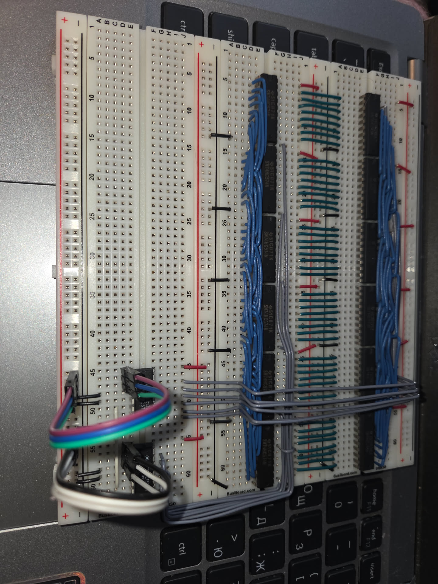
Here’s my progress so far
Bill of Materials
- 74hc245 Octal 3-state transceiver (6)
- 74hc574 3-state Octal D-Type Edge-Triggered Flip-Flop (6)
- 74h138 3-line to 8-line decoder (2)
I’ve uploaded this to reddit.